This is just a rough draft so far. We'd like to make this document really thorough with lots of detailed screenshots and explanations of what everything is used for. Please feel free to join the discussion on how to improve this document here. Or just shoot me an email cdenney@worthingtonassembly.com
A lot of this info could be dead wrong right now. We're still working on it.
Reference URLS
- MIT - Eagle Help - Layers
- Adafruit - An Introduction to Layers in Eagle
- Adafruit - Adding a Silk Screen Outline to your Package
- Sparkfun - Using EAGLE: Board Layout
- Lucidarme - An Introduction to EAGLE
- All About Circuits - Eagle CAD Tips and Tricks
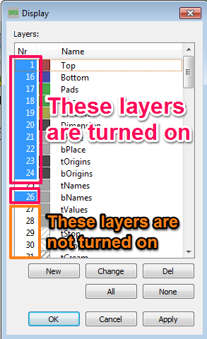
First of all, make sure you know how to access and adjust the layers
After clicking that button you can change whether the layers are viewable or not. The ones that are currently turned on, in order to be displayed by the software, they will have a Blue highlight next to their number. The layers that do not have a Blue highlight are hidden. Just click the number to make them display or not display.
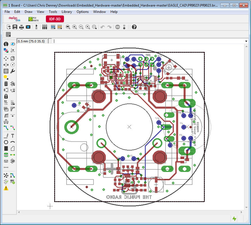
This is what the layout looks like with all of the above layers displayed.
Now that we understand that, let's get into what each layer is used for, what it looks like, and best practices for each layer.
- Top - Top side copper (tracks) - all of the copper on the top of the PCB.
Layer 2 - Route 2 - Inner copper layer (Signal or Supply)
Layer 3 - Route 3 - Inner copper layer (Signal or Supply)
Layer 4 - Route 4 - Inner copper layer (Signal or Supply)
Layer 5 - Route 5 - Inner copper layer (Signal or Supply)
Layer 6 - Route 6 - Inner copper layer (Signal or Supply)
Layer 7 - Route 7 - Inner copper layer (Signal or Supply)
Layer 8 - Route 8 - Inner copper layer (Signal or Supply)
Layer 9 - Route 9 - Inner copper layer (Signal or Supply)
Layer 10 - Route 10 - Inner copper layer (Signal or Supply)
Layer 11 - Route 11 - Inner copper layer (Signal or Supply)
Layer 12 - Route 12 - Inner copper layer (Signal or Supply)
Layer 13 - Route 13 - Inner copper layer (Signal or Supply)
Layer 14 - Route 14 - Inner copper layer (Signal or Supply)
Layer 15 - Route 15 - Inner copper layer (Signal or Supply)
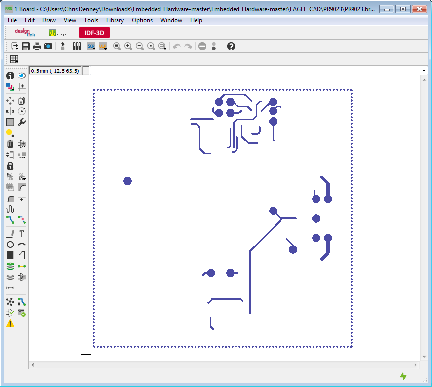
Bottom - Bottom side copper (tracks) - all of the copper on the bottom of the PCB
Pads - Thru-Hole
Vias - Thru-Hole
Unrouted - Airwires (rubberbands) - these are used to help show which pins of which components should be connected to each other. These will begin to disappear as you layout your board. When your layout is complete, none of these should remain.
Dimension Board Outline
tPlace - Top side silkscreen - include reference designators and polarity indicators on this layer
bPlace - Bottom side silkscreen - include reference designators and polarity indicators on this layer
tOrigins - Top side origins - defines the center of a component's placement
bOrigins - Bottom side origins - defines the center of a component's placement
tNames - Top side service print - holds the names for each part on your PCB (ie. R1, U5, C15, etc.)
bNames - Bottom side service print - holds the names for each part on your PCB (ie. R1, U5, C15, etc.)
tValues - Top side component value - holds the value of each part such as 10k for resistors or 1uF for capacitors. This is a great place to specify specific manufacturer's part numbers.
bValues - Bottom side component value - holds the value of each part such as 10k for resistors or 1uF for capacitors. This is a great place to specify specific manufacturer's part numbers.
tStop - Top side solder mask - This defines where soldermask should NOT be. Otherwise soldermask will cover the whole PCB.
bStop - Bottom side solder mask - This defines where soldermask should NOT be. Otherwise soldermask will cover the whole PCB.
tCream - Top side solder paste (stencil). It's important to define where you do and do not want solder paste using these layers.
bCream - Bottom side solder paste (stencil). It's important to define where you do and do not want solder paste using these layers.
tFinish - Top side component finish. Defines what finish material you'd like on your PCB.
bFinish - Bottom side component finish. Defines what finish material you'd like on your PCB.
tGlue - Top side glue mask - defines where you would like glue placed. Useful for components that will experience a lot of stress during the functional use of the PCB, like a switch or connector.
bGlue - Bottom side glue mask - defines where you would like glue placed. Useful for components that will experience a lot of stress during the functional use of the PCB, like a switch or connector. This is especially important for bottom side components that might be too heavy for solder surface tension to hold them in place during the secondary reflow cycle.
tTest - Top side test and adjustments - It defines a testpoint for ICT (In Circuit Test).
bTest - Bottom side test and adjustments - It defines a testpoint for ICT (In Circuit Test).
tKeepout - Top side no-go areas for components. Useful for DRC to make sure two components aren't too close to each other.
bKeepout - Bottom side no-go areas for components. Useful for DRC to make sure two components aren't too close to each other.
tRestrict - Top side no-go areas for traces. Useful for DRC to make sure two components aren't too close to each other.
bRestrict - Bottom side no-go areas for traces. Useful for DRC to make sure two components aren't too close to each other.
vRestrict - No-go areas for via-holes
Drills - Plated thru-holes. Useful for mounting holes where electrical contact needs to be made such as with a ground bolt.
Holes - Non-conducting holes. Useful for mounting holes where no electrical contact should be made.
Milling - Milling layer for internal cutouts
Measures - Measures
Document - General documentation. It's useful to put fabrication notes here such as the thickness of the PCB, stackup specs, soldermask color, silkscreen color, copper weight, material, impedance control specs, surface finish, any other custom requirements.
Reference - Reference marks (fiducial marks) - these are critical for automated assembly and should be included in every design. At least 2 reference marks are necessary but 3 is ideal. We've put together a useful guide on what fiducials are and how they are used.
Skipped
tDocu - Top side part documentation - this can supplement your silkscreen layer for defining characteristics of your PCB. This layer is generally not printed on the PCB itself so make sure your polarity marks and reference designators are still on your tPlace (Layer 21) and bPlace (Layer 22) layers.
bDocu - Bottom side part documentation - this can supplement your silkscreen layer for defining characteristics of your PCB. This layer is generally not printed on the PCB itself so make sure your polarity marks and reference designators are still on your tPlace (Layer 21) and bPlace (Layer 22) layers.


