Design Rule Check - Absolute Limits - 1/2oz Copper
This page will give you the details you need to setup your DRC tool. This page is for the limits of the various rules. You should only use these rules if your design really requires very tight tolerances. If you have the space for it, we recommend not designing your board right up against these rules as it will help fabrication go much smoother and ultimately save you time and money.
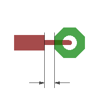
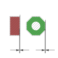
Clearance - Different Signals
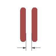
Different Signals Trace to Trace = 5mil (0.127mm)
This is the minimum gap between two traces.
Different Signals Trace to Pad = 8mil (0.203mm)
This is the minimum gap between a trace and an adjacent pad
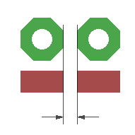
Different Signals Pad to Pad = 10mil (0.254mm)
This is the minimum gap between a pad and an adjacent pad
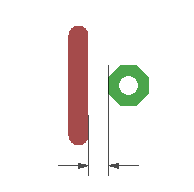
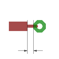
Different Signals Trace to Via = 8mil (0.203mm)
This is the minimum gap between a trace and an adjacent via
Different Signals Pad to Via = 10mil (0.254mm)
This is the minimum gap between a pad and an adjacent via
Different Signals Via to Via = 10mil (0.254mm)
This is the minimum gap between a via and an adjacent via
Clearance - Same Signal
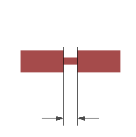
Same Signal SMD Pad to SMD Pad = 6mil (0.152mm)
This is the minimum gap between an SMD Pad and an adjacent SMD Pad on the same signal. This allows a soldermask sliver to be paid between the two pads so that the assembly goes smoothly.
Same Signal SMD Pad to TH Pad = 6mil (0.152mm)
This is the minimum gap between an SMD Pad and an adjacent Thru-Hole Pad on the same signal. This allows a soldermask sliver to be paid between the two pads so that the assembly goes smoothly.
Same Signal SMD Pad to Via = 6mil (0.152mm)
This is the minimum gap between an SMD Pad and an adjacent Via on the same signal. This allows a soldermask sliver to be paid between the two pads so that the assembly goes smoothly.
Distance
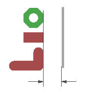
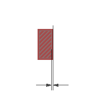
Copper to Edge = 10 mil (0.203mm)
This is the minimum gap between the edge of copper and the edge of your PCB. The edge of the PCB could be outer perimeter of your PCB or a cutout/route inside the PCB itself.
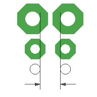
Hole to Hole = 10mil (0.254mm)
This is the minimum gap between the edge of one hole to the edge of another hole. The hole could be plated or non-plated but the rules are the same.
Sizes
Minimum Trace Width = 4mil (0.101mm)
This is the minimum width a trace can be. This only applies for 1oz copper. Thicker copper would increase the minimum value.
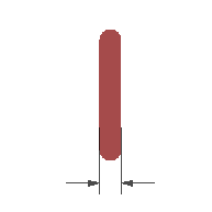
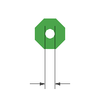
Minimum Drill/Hole =
This is the minimum diameter of a drill/hole.
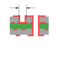
Minimum Micro Via = 10 mils
This is the minimum diameter of a micro via. This value also applies to blind vias that are only one layer deep.
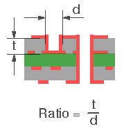
Minimum Blind Via Ratio = 0.5
This is the minimum ratio that a blind via can be (d) as it passes through a certain thickness (t). In other words, if your passing a via through one layer and the layer thickness is 10 mils thick and the minimum blind via ratio is 0.5 then the minimum diameter of via must be 20 mils.
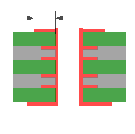
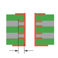
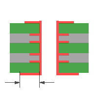
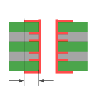
Annular Ring
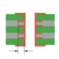
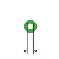
The annular ring for pads should have a minimum and a maximum value set. Having too thin of an annular ring would make the barrel very difficult plate, not to mention soldering the lead in after populating the part would be quite challenging as well. Making them at least 25% as wide as the hole is in diameter is a good rule of thumb. (AutoDesk EAGLE likes to have a maximum value defined for this. Leaving the default 20 mils is fine).
Top Pad Annular Ring
- Min = 10 mils
- Percentage of Hole Diameter = 25%
- Max = 20 mils (when using AutoDesk EAGLE)
Inner Pad Annular Ring
- Min = 10 mils
- Percentage of Hole Diameter = 25%
- Max = 20 mils (when using AutoDesk EAGLE)
Bottom Pad Annular Ring
- Min = 10 mils
- Percentage of Hole Diameter = 25%
- Max = 20 mils (when using AutoDesk EAGLE)
Via Annular Ring - Outer Layers
- Min = 8 mils
- Percentage of Hole Diameter = 25%
- Max = 20 mils (when using AutoDesk EAGLE)
Via Annular Ring - Inner Layers
- Min = 8 mils
- Percentage of Hole Diameter = 25%
- Max = 20 mils (when using AutoDesk EAGLE)
Micro Via Annular Ring - Outer Layers
- Min = 4 mils
- Percentage of Hole Diameter = 25%
- Max = 20 mils (when using AutoDesk EAGLE)
Micro Via Annular Ring - Inner Layers
- Min = 4 mils
- Percentage of Hole Diameter = 25%
- Max = 20 mils (when using AutoDesk EAGLE)
Supply
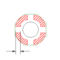
Supply refers to the way that pads are thermally isolated for Supply nets like VCC and GND.
Thermal Isolation = 10 mils
Thermal isolation is very helpful when trying to get a complete solder joint on a thru-hole part. It's also helpful in case any repair needs to be done to that pad as it prevents too much heat from the soldering iron from being carried away from the solder itself and into the PCB.
Masks
Usually you do not want soldermask on top of your copper pads where components need to be soldered. These are called "non-soldermask defined" pads (NSMD), as opposed to "soldermask defined" pads (SMD). The following values only apply to NSMD pads.
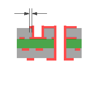
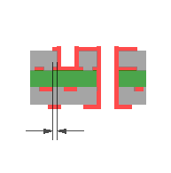
Minimum Soldermask Isolation = 4 mils
This is the gap from the edge of the copper to where the soldermask begins. This area will be left open with bare substrate material (usually FR4).
(AutoDesk EAGLE will call this "Stop". They will also ask for a percentage which you can leave at 100%)
Maximum Soldermask Isolation = 4 mils
If your DRC tool asks for this, it is usually left to the same value as your minimum.
Solder Paste Gap = 0 mils
This is the amount the solder paste is pulled in from the edge of the copper pad for SMT components. We really prefer this value be left at 0 so that the solder paste is defined as the exact same size as the pad itself. We will usually adjust all of these values ourselves when we get the stencil made and leaving them at 0 will help prevent any miscalculations.
Soldermask Over Hole Limit = 30 mils
If you would like to have your vias covered in soldermask (we HIGHLY recommend that you do, unless you have specific requirements for not doing so) then the largest via that can be covered with soldermask would be set to this value. Any via holes larger than this will not be covered with soldermask and left exposed.

